Voltage Levels Control Relays

This circuit proves that microcoprocessors, PCs and the latest ultra-accurate DACs are overkill when it comes to controlling four relays in sequence in response to arising control voltage in the range 2.4 V –12 V. By using equal resistors in ladder network R1-R5, equal intervals are created between the voltages that switch on the relays in sequence. Each resistors drops 1/5th of the supply voltage or 2.4 V in this case, so we get +2.4 V = Re1, +4.8 V = Re2, +7.2 V = Re3, +9.6 V = Re4.

Obviously, these switching levels vary along with the supply voltage, hence the need to employ a stabilised power supply. Looking at the lowest level switching stage, when the control voltage exceeds 2.4 V, IC1 will flip its output to (nearly) the supply level. The resulting current sent into the base of T1 is limited to about 1 mA by R6. With T1 driven hard, relay Re1 is energised by the collector current. Because the BC548 has a maximum collector current spec of 100 mA, the relay coil resistance must not be smaller than 120 ohms.

Circuit diagram:Voltage Levels Control Relays
Voltage Levels Control Relays Circuit Diagram

Nearly all current consumed by the circuit goes on account of the relay coils, so depending on your relays a pretty hefty power supply of up to 500 mA may be required. When dimensioning the ladder network to create the desired switching levels, it is good to remember that the 741 will not operate very well with input voltages below 1.5 V or above 10.5 V, while voltage levels outside the supply range (i.e., negative or above +12 V) are out of the question.

If you do need a switching level in the range 0-1.5 V, consider using an LM324, which contains four opamps in one package. For the high side of the range (10.5 to 12 V), a TL084 or a ‘rail-to-rail’ opamp like the TS924 is required. However, the TS924 cannot be used with supply voltages above 12 V.
Author: Raj. K. Gorkhali - Copyright: Elektor 2004

DMM Fuse Protector

Typically the input protection fuse of your DMM will blow in the middle of a demonstration or an exciting phase of your construction work. Spare fuses are always hard to find, and if available take a lot of time to install. This circuit replaces the fuse by a 500 mA current limiter. When resistor R1 passes about 500 mA, it will drop 0.75 V which is sufficient to switch on T2.

With the buzzer acting as a pull-up resistor (and, of course, as a very loud acoustic warning device), the voltage at the gate of power FET T1 will drop to a level at which the drain-source current is limited to a safe value of about 500 mA. Of course, the excess energy caused by the current limiting action is dissipated by the FET.

Cooling is required in all cases where the dissipation can be expected to exceed about 1-2 watts. After all, without cooling, the voltage allowed to occur across the FET will be just 4V (2 W = 0.5 A × 4 V). Although an IRF740S is indicated in the circuit diagram, almost any power FET may be used.

The popular BUZ10, for example, is a good choice when a lot of power has to be dissipated. If a 12-V mini battery is used then the buzzer should also be a 12-V device. However the circuit will also work fine from the more commonly found (and certainly less expensive) 9-V battery and a matching buzzer. If the latter is not required it is simply replaced by a 10-kΩ resistor.

Floating 9V Supply For DVM Modules

Most commercial DVM modules with an LCD readout are 9-V powered and based on an ICL7106 or similar A-D converter chip. These modules are typically used in laboratory power supplies and other test and measurement equipment where a drop-in solution needs to be found to realize a voltmeter readout. Particularly in power supply units, the LCD module will need to ‘float’ relative to the PSU supply rails, and this inevitably requires a separate 9-volt power supply. In some cases, batteries may be used but these have distinct advantages. The alternative, a 9-V converter effectively powered by the PSU and yet floating, is shown here.

Floating 9V Supply For DVM Modules Circuit Diagram
It is built from the ubiquitous TLC555, LMC555 or 7555) timer IC acting in astable multivibrator configuration producing a 70-kHz square wave fed into a simple rectifier. In essence, capacitors C5 and C6 afford the above mentioned electrical isolation between the PSU supply rails and the LCD module. The old, bipolar NE555 IC should not be used here because it presents a too heavy loads on the converter’s own supply voltage.

Depending on the exact type and brand of the CMOS 555 you’re using, resistor R6 may need to be redimensioned a bit to ensure a supply voltage of about 10 volts at pins 8 and 4 of the chip. At an output voltage of 9.5 V, the maximum output current of the converter s about 1 mA.

Laser Power Supply

If you have ever worked with lasers, you know how fun and interesting it can be, you also know how expensive it can be. The high voltage power supplies for the laser tubes are often more expensive then the tubes themselves. This supply can be built with common parts, most of which you probably already have in your junk box. The secret is the transformer used. It is a common 9V 1A unit, connected backwards for step up.

Parts


Part          

Total Qty.

Description

          
R1   110 Ohm 10W Or Greater Resistor
R2   1Ballast Resistor, See "Notes"
D1, D2, D3   31N4007 Silicon Diode
C1, C2, C3   30.1 uF 2000V Capacitor
T1   19V 1A Transformer
S1   1115V 2A SPST Switch
MISC   1Case, Wire, Binding Posts (for output), Line Cord

Notes

  • T1 is an ordinary 9V 1A transformer connected backwards for step up.
  • R1 MUST be installed on a LARGE heatsink. A good heatsink is the metal case the supply is built in.
  • R2 Protects the laser tube from excess current. It should be soldered directly to the anode terminal on the tube. To find R2, start with a 500K 10W resistor and work down until the tube lights and remains stable.
  • If you have trouble with the tube not starting easily, use a longer anode lead that is wrapped around the tube.
  • Depending on the transformer you use, the circuit may or may not work. I cannot guarantee the operation of this circuit. Build at your own risk. Some transformers contain very few secondary windings which will quickly saturate the core and basically act like a direct short. The more secondary windings (that is, primary in this circuit) the better.

Electronic Fuse for DC Short Circuit Protection

This is an electronic fuse that protects the load against short circuit.

Project Description

Relays must be chosen with a voltage value equals to the input voltage. Don’t omit using the 100uF capacitor with appropriate voltage value with respect to the input voltage. If you can’t provide, you can use C106 instead of BRX46.
Circuit Project: Electronic Fuse for DC Short Circuit Protection by BRX46
You can adjust the current with using 10K potentiometer. If you will use the fuse with very high currents, lower the 0R6 5W resistor value (ex. 0R47, 0R33, 0R22 or 0R1). Watt value of the resistor should be increased also.

Universal DC Power Supply

I didn't realize till the other day that I have never shown a circuit for a standard power supply. Shown below is a supply that will use any of the LM78XX series of voltage regulators. The transformer in the circuit will vary depending on which regulator you use. For voltages from 5 to 12 use a transformer with output of 18vac. With voltages from 15 to 24 use a transformer of 30vac. The first capacitor in the circuit may need to vary if you are supplying more current to the load. Typically it will be 2000uf for every amp of current.

Low Power 12V Transformerless Power Supply

Many circuits can be powered directly from the mains with the aid of a series capacitor (C1). The disadvantage of this approach is that usually only one half cycle of the mains wave-form can be used to produce a DC voltage. An obvious solution is to use a bridge rectifier to perform full-wave rectification, which increases the amount of current that can be supplied and allows the filter capacitor to be smaller.

The accompanying circuit in fact does this, but in a clever manner that uses fewer components. Here we take advantage of the fact that a Zener diode is also a normal diode that conducts current in the forward direction. During one half wave, the current flows via D1 through the load and back via D4, while during the other half wave it flows via D3 and D2. Bear in mind that with this circuit (and with the bridge rectifier version), the zero voltage reference of the DC voltage is not directly connected to the neutral line of the 230-V circuit.
Low Power 12V Transformerless Power Supply

This means that it is usually not possible to use this sort of supply to drive a triac, which normally needs such a connection. However, circuits that employ relays can benefit from full-wave rectification. The value of the supply voltage depends on the specifications of the Zener diodes that are used, which can be freely chosen. C2 must be able to handle at least this voltage.

The amount of current that can be delivered depends on the capacitance of C1. With the given value of 220nF, the current is approximately 15mA. A final warning: this sort of circuit is directly connected to mains voltage, which can be lethal. You must never come in contact with this circuit! It is essential to house this circuit safely in a suitable enclosure.

Under-Over-Voltage Beep for Manual Stabiliser

Manual stabilisers are still popular because of their simple construction, low cost, and high reliability due to the absence of any relays while covering a wide range of mains AC voltages compared to that handled by automatic voltage stabilisers. These are used mostly in homes and in business centres for loads such as lighting, TV, and fridge, and in certain areas where the mains AC voltage fluctuates between very low (during peak hours) and abnormally high (during non-peak hours). Some manual stabilisers available in the market incorporate the high-voltage auto-cut-off facility to turn off the load when the output voltage of manual stabiliser exceeds a certain preset high voltage limit.

The output voltage may become high due to the rise in AC mains voltage or due to improper selection by the rotary switch on manual stabiliser. One of the major disadvantage of using a manual stabiliser in areas with a wide range of voltage fluctuations is that one has to keep a watch on the manual stabiliser’s output voltage that is displayed on a voltmeter and keep changing the same using its rotary switch. Or else, the output voltage may reach the preset auto cut-off limit to switch off the load without the user’s knowledge. To turn on the load again, one has to readjust the stabiliser voltage using its rotary switch. Such operation is very irritating and inconvenient for the user.
Under-Over-Voltage Beep for Manual Stabiliser

This under-/over-voltage audio alarm circuit designed as an add-on circuit for the existing manual stabilisers overcomes the above problem. Whenever the stabiliser’s output voltage falls below a preset low-level voltage or rises above a preset high-level voltage, it produces different beep sounds for ‘high’ and ‘low’ voltage levels—short-duration beeps with short intervals between successive beeps for ‘high’ voltage level and slightly longer-duration beeps with longer interval between successive beeps for ‘low’ voltage level. By using these two different types of beep sounds one can readily readjust the stabiliser’s AC voltage output with the help of the rotary switch.

There is no need of frequently checking voltmeter reading. It is advisable to preset the high-level voltage 10V to 20V less than the required high-voltage limit for auto-cut-off operation. Similarly, for low level one may preset low-level AC voltage 20V to 30V above minimum operating voltage for a given load. The primary winding terminals of step-down transformer X1 are connected to the output terminals of the manual stabiliser. Thus, 9V DC available across capacitor C1 will vary in accordance with the voltage available at the output terminals of the manual stabiliser, which is used to sense high or low voltage in this circuit.

Transistor T1 in conjunction with zener diode ZD1 and preset VR1 is used to sense and adjust the high-voltage level for beep indication. Similarly, transistor T2 along with zener ZD2 and preset VR2 is used to sense and adjust low voltage level for beep indication. When the DC voltage across capacitor C1 rises above the preset high-level voltage or falls below the preset low-level voltage, the collector of transistor T2 becomes high due to non-conduction of transistor T2, in either case. However, if the DC voltage sampled across C1 is within the preset high- and low-level voltage, transistor T2 conducts and its collector voltage gets pulled to the ground level.

These changes in the collector voltage of transistor T2 are used to start or stop oscillations in the astable multivibrator circuit that is built around transistors T3 and T4. The collector of transistor T4 is connected to the base of buzzer driver transistor T5 through resistor R8. Thus when the collector voltage of transistor T4 goes high, the buzzer sounds. Preset VR3 is used to control the volume of buzzer sound. In normal condition, the DC voltage sampled across capacitor C1 is within the permissible window voltage zone. The base of transistor T3 is pulled low due to conduction of diode D2 and transistor T2.

As a result, capacitor C2 is discharged. The astable multivibrator stops oscillating and transistor T4 starts conducting because transistor T3 is in cut-off state. No beep sound is heard in the buzzer due to conduction of transistor T4 and non-conduction of transistor T5. When the DC voltage across capacitor C1 goes above or below the window voltage level, transistor T2 is cut off. Its collector voltage goes high and diode D2 stops conducting. Thus there is no discharge path for capacitor C2 through diode D2. The astable multivibrator starts oscillating. The time period for which the beep is heard and the time interval between two successive beeps are achieved with the help of the DC supply voltage, which is low during low-level voltage sampling and high during high-level voltage sampling.

The time taken for charging capacitors C2 and C3 is less when the DC voltage is high and slightly greater when the DC voltage is low for astable multivibrator operation. Thus during low-level voltage sensing the buzzer beeps for longer duration with longer interval between successive beeps compared to that during high-voltage level sensing. This circuit can be added to any existing stabiliser (automatic or manual) or UPS to monitor its performance.

High Low Voltage Cutout Without Timer

This inexpensive circuit can be connected to an air-conditioner/fridge or to any other sophisticated electrical appliance for its protection. Generally, costly voltage stabilizers are used with such appliances for maintaining constant AC voltage. However, due to fluctuations in AC mains supply, a regular ‘click’ sound in the relays is heard. The frequent energisation/de-energisation of the relays leads to electrical noise and shortening of the life of electrical appliances and the relay/stabilizer itself. The costly yet fault-prone stabiliser may be replaced by this inexpensive high-low cutout circuit with timer.

The circuit is so designed that relay RL1 gets energised when the mains voltage is above 270V. This causes resistor R8 to be inserted in series with the load and thereby dropping most of the voltage across it and limiting the current through the appliance to a very low value. If the input AC mains is less than 180 volts or so, the low-voltage cut-off circuit interrupts the supply to the electrical appliance due to energisation of relay RL2. After a preset time delay of one minute (adjustable), it automatically tries again. If the input AC mains supply is still low, the power to the appliance is again interrupted for another one minute, and so on, until the mains supply comes within limits (>180V AC).

The AC mains supply is resumed to appliance only when it is above the lower limit. When the input AC mains increases beyond 270 volts, preset VR1 is adjusted such that transistor T1 conducts and relay RL1 energises and resistance R8 gets connected in series with the electrical appliance. This 10-kilo-ohm, 20W resistor produces a voltage drop of approximately 200V, with the fridge as load. The value and wattage of resistor R8 may be suitably chosen according to the electrical appliance to be used. It is practically observed that after continuous use, the value of resistor R8 changes with time, due to heating. So adjustment of preset VR1 is needed two to three times in the beginning.
High Low Voltage Cutout Without Timer

But once it attains a constant value, no further adjustment is required. This is the only adjustment required in the beginning, which is done using a variac. Further, the base voltage of transistor T2 is adjusted with the help of preset VR2 so that it conducts up to the lower limit of the input supply and cuts off when the input supply is less than this limit (say, 180V). As a result, transistor T3 remains cut off (with its collector remaining high) until the mains supply falls below the lower limit, causing its collector voltage to fall. The collector of transistor T3 is connected to the trigger point (pin 2) of IC1. When the input is more than the lower limit, pin 2 of IC1 is nearly at +Vcc.

In this condition the output of IC1 is low, relay RL2 is de-energised and power is supplied to the appliance through the N/C terminals of relay RL2. If the mains supply is less than the lower limit, pin 2 of IC1 becomes momentarily low (nearly ground potential) and thus the output of IC1 changes state from ‘low’ to ‘high’, resulting in energisation of relay RL2. As a result, power to the load/appliance is cut off. Now, capacitor C2 starts charging through resistor R6 and preset VR3. When the capacitor charges to (2/3)Vcc, IC1 changes state from ‘high’ to ‘low’. The value of preset VR3 may be so adjusted that it takes about one minute (or as desired) to charge capacitor C1 to (2/3)Vcc.

Relay is now de-energised and the power is supplied to the appliance if the mains supply voltage has risen above the lower cut-off limit, otherwise the next cycle repeats automatically. One additional advantage of this circuit is that both relays are de-energised when the input AC mains voltage lies within the specified limit and the normal supply is extended to the appliance via the N/C contacts of both relays.

Soft Start For Switching Power Supply

Switching power supply whose output voltage is appreciably lower than its input voltage has an interesting property: the current drawn by it is smaller than its output current. However, the input power (UI) is, of course, greater than the output power. There is another aspect that needs to be watched: when the input voltage at switch-on is too low, the regulator will tend to draw the full current.

When the supply cannot cope with this, it fails or the fuse blows. It is, therefore, advisable to disable the regulator at switch-on (via the on/off input). until the relevant capacitor has been charged. When the regulator then starts to draw current, the charging current has already dropped to a level which does not overload the voltage source.

The circuit in the diagram provides an output voltage of 5 V and is supplied by a 24 V source. The regulator need not be disabled until the capacitor is fully charged: when the potential across the capacitor has reached a level of half or more of the input voltage, all is well. This is why the zener diode in the diagram is rated at 15 V. Many regulators produced by National Semiconductor have an integral on/off switch, and this is used in the present circuit.

The input is intended for TTL signals, and usually consists of a transistor whose base is accessible externally. This means that a higher switching voltage may be applied via a series resistor: the value of this in the present circuit is 22 kΩ. When the voltage across the capacitor reaches a level of about 17 V, transistor T1 comes on, whereupon the regulator is enabled.

Upgrade Your USB Hub

Problems can arise with USB hubs that are powered from a PC when gadgets plugged into them draw too much current. This is often the case with devices fitted with USB cables that are too long or too thin, causing voltage drop. There’s no need to scrap your old USB hub, however, if you upgrade it using this little circuit and an external power supply. Just cut the 5-V power wire of the USB cable inside the hub and solder a diode (D1) in the pass-through direction. Now connect the 5 V wire from the external power supply to the cathode of this diode. D1 prevents any current from the power supply from flowing back into the PC.

High-Power Car Battery Eliminator

To operate car audio (or video) system from household 230V AC mains supply, you need a DC adaptor. DC adapters available in the market are generally costly and supply an unregulated DC. To overcome these problems, an economical and reliable circuit of a high-power, regulated DC adaptor using reasonably low number of components is presented here. Transformer X1 steps down 230V AC mains supply to around 30V AC, which is then rectified by a bridge rectifier comprising 5406 rectifier diodes D1 through D4. The rectified pulsating DC is smoothed by two 4700µF filter capacitors C1 and C2.

The next part of the circuit is a series-transistor regulator circuit realised using high-power transistor 2N3773 (T1). Fixed-base reference for the transistor is taken from the output pin of 3-pin regulator IC1 (LM 7806). The normal output of IC1 is raised to about 13.8 volts by suitably biasing its common terminal by components ZD1 and LED1. This simple arrangement provides good, stable voltage reference at a low cost. LED1 also works as an output indicator. Finally, a crowbar-type protection circuit is added. If the output voltage exceeds 15V due to some reason such as component failure, the SCR fires because of the breakdown of zener ZD2.
High-Power Car Battery Eliminator

Once SCR fires, it presents a short-circuit across the unregulated DC supply, resulting in the blowing of fuse F1 instantly. This offers guaranteed protection to the equipment connected and to the circuit itself. This circuit can be assembled using a small general-purpose PCB. A good-quality heat-sink is required for transistor T1. Enclose the complete circuit in a ready made big adapter cabinet as shown in the figure.

Adjustable 3 Ampere Regulator

By combining a common 78L05 with an integrated audio amplifier of the type TDA2030, an adjustable voltage regulator can be constructed in a very simple manner that works very well. The output voltage is adjustable up to 20 V, with a maximum current of 3 A.

Since the TDA2030 comes complete with a good thermal and short-circuit protection circuit, this adjustable regulator is also very robust. As illustrated by the schematic, the design of this circuit is characterized by simplicity that is hard to beat. In addition to the two ICs, the regulator contains actually only two potentiometers and a few capacitors.

Adjustable 3 Ampere Regulator Circuit DiagramThe adjustment is done by first turning potentiometer P1 to maximum (wiper to the side of the 78L05) and subsequently turning trimpot P2 until the desired maximum output voltage is reached. P1 is then used to provide a continuously adjustable voltage between this maximum and nearly zero volts. At relatively small output currents there are no specific requirements regarding the cooling. However, when the output current exceeds 1 A, or if the input to output voltage difference is quite large, the amplifier IC has to dissipate too much power and a small heatsink is certainly appropriate.

Solar Panel Voltage Regulator

Our energy-hungry and environmentally aware society has been slow to make good use of the sun's "free" power. But now it's finally taking off. Using the sun's heat directly, for cooking and other applications, is already a common and popular technology in countries that have good weather. Hot-water panels are nowadays used in many parts of the world, in combination with a gas or electric powered water heater to help out when the weather doesn't help. But at the same time, electric solar panels are still expensive, justifying their use only as a novelty, or in locations where little power is needed, and bringing in commercial power would be even more expensive.

A solar electric power system needs panels for generation, batteries for storage, a regulator to keep the batteries within a safe operating range, and in some cases a power converter for AC output. For those who need to set up a few panels for a summer cottage, a boat, a remote mountaintop installation, or whatever, I'm herewith providing a version of the regulator circuit that I have used in a lot of such installations.

Such a solar panel regulator should perform at least two operations: The obvious one is protecting the battery from overcharge at times of strong sun and little consumption, and the other is protecting it from excessive discharge in bad weather conditions. Both overcharge and deep discharge are harmful to a battery.

Circuit Project: Solar Panel Voltage RegulatorFor regulating a solar panel's output, there are several possible ways. A linear series regulator can be used, but has the disadvantage of causing some voltage drop and having some internal power consumption at times when the sun is weak and the load is heavy. It's much better to use a shunt regulator, which is inactive at such times, and springs to life only when there is excess energy. For this reason, most solar panel regulators use the shunt scheme, the one presented here being no exception.

But such shunt regulators come in two flavors: Most commercial units are ON-OFF regulators. That means, they have a simple switch device, most often a transistor or MOSFET, sometimes even just a relay, that stays off until the battery reaches over voltage, and then switches in, shorting out the panel until the battery voltage has dropped off. Then the full panel current is switched on again. The only advantage of this method is that's cheap. The power switch operates with very low power dissipation, allowing a small, low cost construction.

But the disadvantages of this system are major: The voltage output is all the time fluctuating between about 13 and 14.5V. The battery is cycling between getting overcharge and having to deliver all the load current, which severely reduces the battery's lifetime. And in the event of battery disconnection or failure, the regulator cycles quickly, applying pulses of full panel voltage to the output, which can destroy sensitive equipment powered by the system!

The circuit presented here uses linear shunt regulation. Simply spoken, it burns off all excess energy from the panel, keeping output voltage constant. At times when the solar panel output is equal or greater than the load, and the battery is fully charged, the load gets its power from the panel, while the battery rests at full charge. Five years battery lifetime are entirely normal with this system, while the same batteries last only two to three years when used with pulsing regulators!

The second responsibility of the regulator is watching over the battery voltage, and dropping off the load when the battery gets discharged too much. Lead batteries are severely damaged by deep discharges, so it's far preferable to drop off the load, then to have the battery die in a bad weather spell. This regulator is designed for 12V systems employing panels of up to 7A total current, and loads of not over 20A. It can be easily modified for greater currents.

U1A compares an adjustable sample of the present battery voltage to a 5V reference from a highly stable source. According to the result, it controls the power transistors Q1 and Q2, which shunt off the excess power generation from the panel. A diode (D1) avoids battery voltage to go back to the panel under no-light condition. To avoid imprecise voltage control due to varying diode drop, the sample is taken from the battery side, even if this means a very small power waste.

The power resistors R1 and R2 are dimensioned in such a way that under maximum shunting, these resistors will dissipate almost all power (about 100W total), leaving the transistors running cool. The highest dissipation in the transistors happens when the regulator is dissipating half of the panel output; in this case, each transistor will dissipate about 12W.

U1B is a Schmitt trigger that compares the battery voltage to the same stable reference of the other section, but for another purpose: It controls the load switch Q3. This circuit will disconnect the load if the battery gets close to deep discharge, and reconnect it only when recharge is well underway. The negative side of the load is switched, simply because N-channel MOSFETs are much cheaper and better than P-channel ones.

Component notes:

D1 can be any diode that can safely survive the panel's current. If the panel has a very low voltage output (less than 33 cells in series), it is an advantage to employ a Schottky diode in this place. Q1 and Q2 are common power Darlington transistors. They need to be heatsinked for safe long-term operation at the 12 Watt dissipation level. That's easy enough to do, but many newcomers misjudge how much thermal resistance is introduced by a mica insulator! Plan on 1K/W thermal resistance inside each transistor, two times as much in the insulator (if you use any), and 370K safe junction temperature. For typical environmental conditions, this makes you need a heatsink having a thermal resistance of about 1.3K/W. If it is larger, you get more safety margin.

R1 and R2 will have to be made by combining a number of power resistors in parallel. Yes, you need to make two resistor arrays of 4 Ohm, 80W each! This 80W figure includes a reasonable safety margin. These resistors will produce a lot of heat, and you may cook your coffee on them! Be sure to mount them in such a way that they have lots of ventilation, and that the heat from them will not reach the other components. R3 and R4 may to have be built from parallel combinations too, because of the low value of only 0.15 Ohm.

U2 is a voltage reference IC. You cannot replace it by a standard Zener diode! Zeners are much too unstable! If you can't find this chip locally, you may use the ubiquitous 7805 regulator instead, but the power drain from the battery will be higher. In this case, of course you don't need R8, but you would need a 1uF capacitor at the 7805 output. Q3 is a power MOSFET that has a very low Rds(on). You may use a different one, provided that it has a resistance that's low enough for your application. You may use several in parallel. The one I used has low loss even at loads of 20A, and can handle much more!

Calibration:

Once the circuit is assembled, calibration is quite easy. Connect the panel, leave the battery and load disconnected. With a nice sun on the panel, adjust RV1 for the desired voltage at the battery output. I recommend 13.8V for sealed batteries, and 14 to 14.2V for open cell ones, to which water can be added if necessary.

Now you need either a variable power supply connected to the battery lines, or some kind of variable load. You may also use your panel as variable power supply, by tilting it away from the sun while a fixed load is connected to the battery lines. The idea is to adjust the voltage at the battery lines to the desired shut-off value (I recommend 11.5V), and then move RV2 until Q3 shuts off, as indicated by a voltmeter across the load output, a 12V light bulb, or whatever you can use to detect it. After Q3 has shut off, increase the voltage across the battery lines and see at which level Q3 switches on again. This should happen above 12.6 and below 13.4 V. You may have to retouch RV2 and look for a compromise between ON and OFF voltages. If your components are not too much out of value, then both potentiometers should have ended up reasonably close to the center position.

Using more panels:

You can use this regulator for larger installations. Simply add one group like R1-Q1-R3 for each additional 3.5A panel, and use a diode for D1 that handles the total current. Remember that large diodes need heat sinks! U1A can drive at least 8 such transistors. If you intend to build a really large system, you may want to add an emitter follower between U1A and the power transistors. If you need to handle large load currents, you can place as many MOSFETs in parallel as you need. There is no practical driving limitation in this case. [via]

Low-Drop 5V Regulator

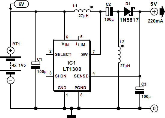
A 4-cell pack is a convenient, popular battery size. Alkaline manganese batteries are sold in retail stores in packs of four, which usually provide sufficient energy to keep battery replacement frequency at a reasonable level. Generating 5 V from four batteries is, however, a bit tricky. A fresh set of four batteries has a terminal voltage of 6.4 V, but at the end of their life, this voltage is down to 3.2 V. Therefore, the voltage needs to be stepped up or down, depending on the state of the batteries. A flyback topology with a costly, custom designed transformer could be used, but the circuit in the diagram gets around the problem by using a flying capacitor together with a second inductor.
Low-Drop 5V Regulator

The circuit also isolates the input from the output, allowing the output to go to 0 V during shutdown. The circuit can be divided conceptually into boost and buck sections. Inductor L1 and switch IC1 comprise the boost or step-up section, and inductor L2, diode D1 and capacitor C3 form the buck or step-down section. Capacitor C2 is charged to the input voltage, Vin, and acts as a level shift between the two sections. The switch toggles between ground and Vin+Vout , while the junction of L2, C2 and D1 toggles between –Vin and Vout +Vd1. Efficiency is directly related to the quality of the capacitors and inductors used.

Better quality capacitors are more expensive. Better quality inductors need not cost more, but normally take up more space. The Sanyo capacitors used in the prototype (C1–C3) specify a maximum ESR (effective series resistance) of 0.045 ½ and a maximum ripple current rating of 2.1 A. The inductors used specify a maximum DCR (direct current resistance) of 0.058 ½. Worst-case r.m.s. current through capacitor C2 occurs at minimum input voltage, that is, 400 mA at full load with an input voltage of 3 V.

Dual Opamp Buffered Power Supply

There will be instances where the currents from each supply will be unequal. Where this is the case, the resistor divider is not sufficient, and the +ve and -ve voltages will be unequal. By using a cheap opamp (such as a uA741), a DC imbalance between supplies of up to about 15mA will not cause a problem. However, we can do better with a dual opamp (which will cost the same or less anyway), and increase the capability for up to about 30mA of difference between the two supplies.

Circuit diagram:Dual Opamp Buffered Power Supply
Dual Opamp Buffered Power Supply Circuit Diagram
Author: ESP

RS232 Voltage Regulator

There are many small applications where it would be preferable to power a device directly from an RS232 (V.24) interface, avoiding a mains power supply. Most ICs require 5 V, and the interface can provide a current of around 8 mA, almost all of which would be consumed by a readily-available voltage regulator, leaving nothing for the actual circuit. Using just four transistors we can construct a voltage regulator with current limiting which will allow us to draw more than the permitted 8 mA from an RS232 interface without damaging it. The example circuit in is configured for an output voltage of 5 V from an input voltage of at least 8 V, and a short-circuit current of 19 mA.

The current drawn by the regulator itself is only 0.2 mA. The circuit appears very simple, but it is more cunning than it looks. Few people appreciate what a handy device the transistor is. To meet the requirements for the circuit, the gains of the transistors need to be controlled carefully. Here only B-class devices are used, which have a gain of between about 220 and 280. Diodes D1 to D3 extract the positive voltage from the serial interface. Current limiting is achieved via resistor R1 and transistor T1. As soon as the voltage across the resistor reaches 0.7 V (at 18 mA with R1 = 39 Ω) the transistor turns on and thus turns off the output voltage by turning off T2. The output voltage of 5 V is set by Zener diode D4.

RS232 Voltage Regulator Circuit Diagram

Note that the output voltage is only approximate: beware when using components which have narrow supply voltage tolerances. When the Zener diode voltage and the voltage across transistor T4 are added together, the total is 5.8 V. However, because of T3, the diode is operating at a low current and the actual threshold for T4 is 4.9 V. The main regulation loop is built around R2 and T2. The high value of R2 (1.5 MΩ) is important, since this limits the maximum current through T2. At the output we would like to be able to draw a maximum current of 19 mA. The base of T2 must therefore be supplied with exactly 1/220 (the gain of the transistor) of 19 mA, and likewise the current into the base of T3 should be just 1/220 of 80 µA. With an input voltage of 9 V the voltage drop across R2 will be 3.3V, and so a current of 2.2 µA will flow. Transistor T3 multiplies this current by 220 to 0.5 mA, which is also the minimum quiescent current of the circuit.
Author: M. Müller
Copyright: Elektor Electronics

Negative-Output Switching Regulator

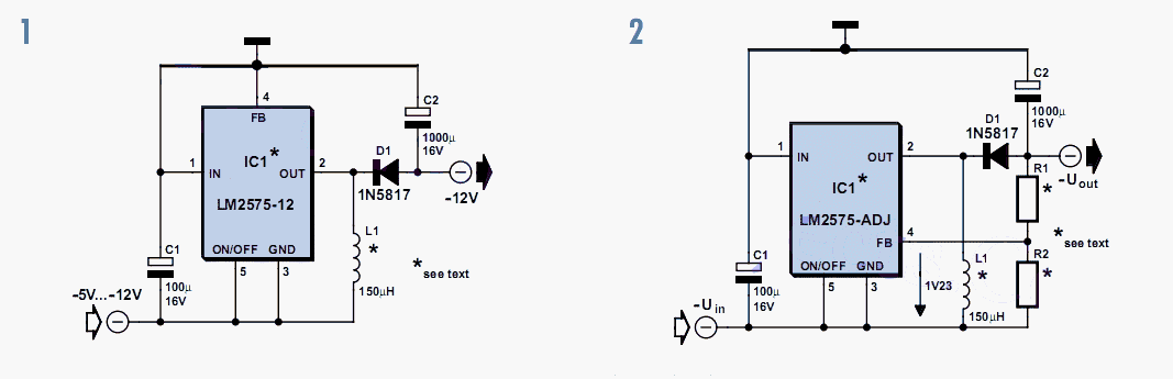
There are only a limited number of switching regulators designed to generate negative output voltages. In many cases, it’s thus necessary to use a switching regulator that was actually designed for a positive voltage in a modified circuit configuration that makes it suitable for generating a negative output voltage. The circuit shown in Figure 1 uses the familiar LM2575 step-down regulator from National Semiconductor (www.national.com). This circuit converts a positive-voltage step-down regulator into a negative-voltage step-up regulator. It converts an input voltage between –5 V and –12 V into a regulated –12-V output voltage.

Note that the output capacitor must be larger than in the standard circuit for a positive output voltage. The switched current through the storage choke is also somewhat higher. Some examples of suitable storage chokes for this circuit are the PE-53113 from Pulse (www.pulseeng.com) and the DO3308P-153 from Coilcraft (www.coilcraft.com). The LM2575-xx is available in versions for output voltages of 3.3V, 5 V, 12 V and 15 V, so various negative output voltages are also possible. However, you must pay attention to the input voltage of the regulator circuit. If the input voltage is more negative than –12 V (i.e., Vin < –12 V), the output voltage will not be regulated and will be lower than the desired –12 V.
Negative-Output Switching Regulator

The LM2575 IC will not be damaged by such operating conditions as long as its maximum rated input voltage of 40 V is not exceeded. High voltage (HV) types that can withstand up to 60 V are also available. Although the standard LM2575 application circuit includes circuit limiting, in this circuit the output current flows via the diode and choke if the output is shorted, so the circuit is not short-circuit proof.

 This can be remedied by using a Multifuse (PTC) or a normal fuse. There is also an adjustable version of the regulator with the type designation LM2575-ADJ (Figure 2). This version lacks the internal voltage divider of the fixed-voltage versions, so an external voltage divider must be connected to the feedback (FB) pin. The voltage divider must be dimensioned to produce a voltage of 1.23 V at the FB pin with the desired output voltage. The formula for calculating the output voltage is:

V out = 1.23 V × (1 + [R1 ÷ R2])

The electrolytic capacitors at the input and output must be rated for the voltages present at these locations.

USB 5V to 12V DC-DC Step-Up Converter by LT1618

This is a 5V to 12V DC-DC step-up (boost) converter circuitry that is especially ideal for the USB powered applications. First of all a USB port has two current supply modes. Before detecting the connected device, it supplies maximum 100mA to the load. After recognizing the device, it increases the output current up to 500mA. In this circuit, controller (LT1618) also provides two input current modes. 100mA and 500mA input modes can be selected by the user.

USB 5V to 12V DC-DC Step-Up Converter by LT1618
Output currents are limited due to the increased potential difference at the output. When the demand of the load increases, output voltage will start to decrease. For example, if the circuit operates in the 100 mA input mode, when the load is 35 mA, the output voltage will be kept at 12V. But if the load increases to 50 mA,output voltage will reduce to 8V to maintain the constant 100 mA input current.

Adjustable Symmetrical Power Supply Using LM317 and LM337

The circuit was designed to provide an adjustment with a power supply that is symmetrically designed while providing a voltage range of 1.25V to 30V at 1A current. LM317 – an adjustable 3-terminal positive voltage regulator capable of supplying in excess of 1.5A over an output voltage range of 1.2V to 37V and requires only two external resistors to set the output voltage due to its internal current limiting, thermal shutdown and safe area compensation, making it essentially blow-out proof LM337 – an adjustable 3-terminal positive voltage regulator capable of supplying in excess of 5A used as battery chargers, constant current regulators, and adjustable power supplies due to its features such as protected output from short circuit, product enhancement tested, current limit constant with temperature, guaranteed thermal regulation, adjustable output down to 1.2V, guaranteed 5A, and guaranteed 7A peak output current.

Adjustable Symmetrical Power Supply Using LM317 and LM337

The circuit will serve as a voltage converter with an input voltage of 35 V to produce an output voltage of 1.25 V to 30 V. The positive voltage is being handled by LM317 IC while the negative voltage is handled by LM337. The circuit can provide an output current of 1 A. During the production of 1 A current, the regulator is dissipating too much heat and without the presence of a heatsink, the regulator may get damaged.

Using these types of regulators provide features such as low noise and low price in the market. It can be made operational even with few components used. The only disadvantage that it will impose is the poor conversion efficiency. With the output of 35 V to 5 V, the efficient ratio of the output power with the input power is less than 42%. This is the reason why the switching regulator became cheap recently although the number of external components to be connected is minimally increased.

These regulators will work with better efficiency when used in case where current is more than 1A for more than 15 V and 0.4 A for less than 15 V from the power supply. Each regulator is adjusted for single positive and negative voltage output using the 10K ohms potentiometers RV1 & RV2. For dual outputs, a dual connected potentiometer RV3 is made to operate by switch S1. The visual indication on the voltmeter V1 is shown using the switch S2.
  • R1-2=270ohms
  • R3-4=2.2Kohms
  • R5-6=10Kohms
  • C1-5=100uF/63V
  • C2-4=100nF/100V
  • C3-8=10uF/25V
  • C6-10=100uF/63V
  • C7-9=100nF/100V
  • RV1-2=10Kohms Lin.
  • RV3=2X10Kohms Lin.
  • IC 1=LM 317T
  • IC 2=LM 337T
  • D1-2=1N4001
  • D3-4=1N4001
  • L1-2=LED 3mm
  • F1-2=1A slow Blow Fuse
  • S1-2=2X ON-ON SW
  • V1=0-30V DC Voltmeter
The adjustable symmetrical power supply is suitable to be used in audio amplifiers, microphone amplifiers, op-amp applications, impedance converters and other devices that require regulated positive and negative DC supply, since the output current is 1 A.